
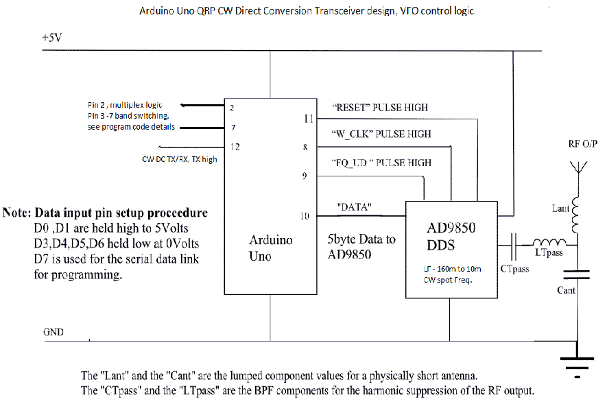
The above circuit diagram is one of a “Arduino Uno CW QRP Direct Conversion Transceiver VFO design”. The AD9850 DDS VFO synthesiser is serial programmed by the Arduino Uno development board, the Arduino Uno also providing the band switching control logic. The circuit diagram to the left, shows the transistor switching logic circuit. By using a combination of NPN and PNP transistors, the multipliex enable of “pin 2” of the Arduino Uno, would select switch between 160m or 17m band. The “pin 3” is the control pin for the 160m and 17m bands, such that pins 4 to 7 thus control with pin 2, the remainder band switching requirements.
// band switching definitions
Pin 2 = multiplex either logic low or high
Pin 3 = topband ( pin 2 low ) / 17m ( pin 2 high )
Pin 4 = 80m ( pin 2 low ) / 15m ( pin 2 high )
Pin 5 = 40m ( pin 2 low ) / 12m ( pin 2 high )
Pin 6 = 30m ( pin 2 low ) / 10m ( pin 2 high )
Pin 7 = 20m ( pin 2 low )/ MF “475KHz” ( pin 2 high )
The keyboard control functions for the CW program are:
[ is TX;
] is RX;
+ ( plus key) is 50HZ increment of the dial frequency
- ( minus key ) is 50HZ increment of the dial frequency
? Toggles the HF bands from 160m to 10m and MF (475KHz)
 VFO Circuit
The Arduino Uno program design for the VFO utiltises a CW full-break-in mode of transceiver design. The CW keyed break-in is conducted during the individual Morse code dot and dash components, as awell in-between the whole message character during the space breaks. The RIT shift on TX mode is down 600Hz, CW as an LSB signal.